What’s an SoC? Defining system-on-chip is harder than you think.
As gadgets get more advanced, the technology inside them has been subtly changing. Not too long ago, microcontrollers were the mainstay of most battery-powered gadgets and appliances around the home. But over the last decade or so this has started to shift, and ever more devices are now based upon system-on-chips (SoCs). But what exactly is this new class of chip, where did it come from, and how does it differ from its predecessors?
A system-on-chip is actually surprisingly difficult to define.
At one end of the spectrum it can be considered something like a souped-up microcontroller (MCU). Somewhere in the middle you might find obscure chips used in specialist media and wireless communications. And at the other end, it can be thought of as an entire desktop computer squeezed into a single chip.
The most general definition is that it’s a microprocessor and all its supporting circuitry on the same piece of silicon. The trouble is, that’s pretty similar to the definition of a microcontroller.
Come On, Really? I’ll Just Google “SoC Wiki”…
Go ahead. If you do google “soc wiki” you’ll see it defined as:-
an integrated circuit … that integrates all components of a computer or other electronic system.
That first sentence is surprisingly all-encompassing! It goes on:-
These components typically include a central processing unit (CPU), memory, input/output ports and secondary storage – all on a single substrate. It may contain digital, analog, mixed-signal, and often radio frequency signal processing functions, depending on the application
And that’s the problem with defining exactly what an SoC is. It can contain just about anything. It’s almost exactly like trying to define what an integrated circuit is. So let’s start right there.
What is an Integrated Circuit?
This might sound like a basic question, but they’ve been around for so long that you might not think too hard about the answer.
The definition of an integrated circuit is an electronic circuit on a piece of silicon. This is the actual silicon chip. But the silicon itself is extremely fragile, so it’s always embedded in some kind of package, generally epoxy, plastic or ceramic, normally with lettering indicating the part number, manufacturer, and so on.
In everyday usage, the entire packaged device is also called a “chip”.
Hybrid integrated circuits (HICs)
Before integrated circuits became commonplace, engineers sometimes built hybrid systems with individual, discrete components packaged together in close configurations, often sealed in epoxy resin. Partly this was for robustness, and partly for secrecy. After ICs became widespread, engineers added ICs into these epoxy “potted” packages.
Today they are usually called hybrid integrated circuits (HICs). A common place you see them is in power supply applications such as DC-DC converters, and also in brushless motor speed controllers such as those found in drones.
Much of the electronics used in the early space missions was built this way. Small integrated circuits were available, but not advanced ones such as microprocessors. Space engineers heavily used (and still use) resin potting to prevent the circuits from begin shaken apart by the extreme forces of a rocket launch.
Hybrid Devices: MCMs, SiPs, PoPs
What has all this got to do with SoCs?
Well, there is a whole area of highly-integrated, hybrid devices that pave the way to full-fledged SoCs. They follow this heritage of cramming disparate circuits into sealed packages.
Multi-chip modules (MCMs) are very common. Lots of specialist circuits are built using multiple chips and discrete components on a small PCB with the same footprint as another chip package. Often this module is used as a drop-in replacement for an older or more expensive part. Some Intel and AMD processor “chips” were not in fact chips but actually multi-chip modules.
So MCMs at one extreme can be considered nothing more than very complex PCBs, but in more advanced examples the components, including entire microprocessors, are actually integrated onto a single substrate.
And just because an integrated circuit is a silicon chip sealed inside a package, engineers realised very early on that there’s no reason why they couldn’t put multiple, but separate silicon dies into the same package. It would reduce the overall circuit size and power consumption, and increase reliability since the interconnects would be potted inside the package rather than on the PCB.
These devices are called system-in-packages (SiPs).
A more recent variant of the SiP is where the constituent silicon dies are actually designed with regular connection points so they can be vertically stacked on top of one another. This arrangement is called a package-on-package (PoP). A common use case would be for a microprocessor die to be vertically stacked with a RAM die.
Things get more complex when SoCs are combined into PoPs. For example, every version of Apple’s iPhone and iPad has included a main “processor” package-on-package consisting of an ARM-based SoC vertically stacked with a RAM chip.
A Practical Definition of an SoC
So where is this veritable mess of definitions does the system-on-chip fit?
The general descriptions at the top of this article have already failed us, so I’ll attempt to provide a definition of a system-on-chip in practical terms.
One thing is clear: the entire system must fit on a single silicon die.
But that still leaves the problem of the microcontroller. How is an SoC different?
First of all, let’s look at where they’re used.
The most common places you’ll find an SoC are in your smartphone, tablet, smart TV, and voice assistant. Inside your computer you may now find SoCs in several places, including the hard drive, network cards and graphics cards. And in many cases, especially with ultra-mobile laptops, the main processor chip may in fact be a SoC with several CPU cores and an integrated graphics processing unit (GPU).
There is also a plethora of ultra-cheap single-board computers available, such as the Raspberry Pi and Beagle Bone. Most of them are based around SoCs.
How do these applications differ from those using MCUs?
The simple answer, today, is computing power. SoCs are only found in devices that need them. Your fridge, washing machine and toaster are probably still using tried-and-tested MCU technology because it’s small, cheap, reliable and relatively easy to code.
So we can consider an SoC to be any relatively high-powered integrated computing system in a single package.
Of course, relative is a key word here. The computing power of microcontrollers will always continue to rise, so for a device to be classed as an SoC it needs to put some clear blue water between itself and an MCU.
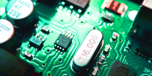
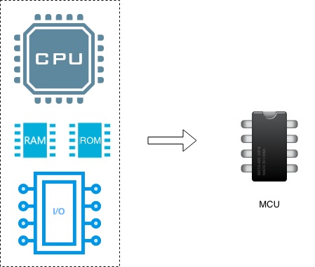
Below are two diagrams showing the relative levels of integration between MCUs and SoCs.
First, a typical microcontroller:-
And next a typical SoC:-
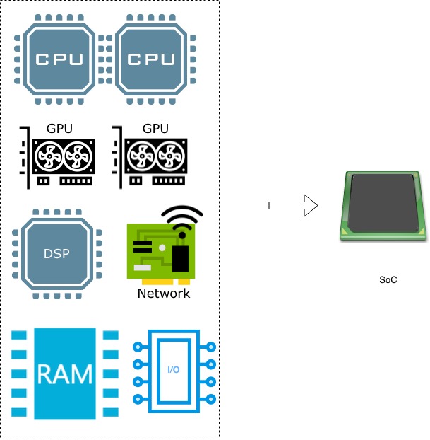
Hopefully this illustrates that for practical purposes, the distinction between an MCU and an SoC is one of complexity.
So now you have a working definition of an SoC. But where did they come from?
A Brief History of the SoC
A lot of the history of the SoC is not public knowledge because much of the early development was done in the research and development labs of private companies. Intellectual property laws and NDAs prevented much of this work becoming public. Many companies developing the technology that would later come to be called SoCs were at the cutting edge of the telecoms industry. They were developing silicon for other companies, not for general sale to design engineers, so the chips they produced tended to have obscure codenames and part numbers that weren’t listed in publicly available catalogues.
The 1970s: Origin of the System-on-Chip
The goal of SoC technology is miniaturisation. So perhaps it should be no surprise that its origins date back to the early 1970s and the new era of the digital watch.
The first ever LED wristwatch, the Hamilton Pulsar, was announced in 1970. Costing a cool $2,100, only James Bond could afford one. In order to produce it, 44 logic ICs had to be reduced into a single chip, but it was not actually a complete system because some of the LED driving circuitry was too large.
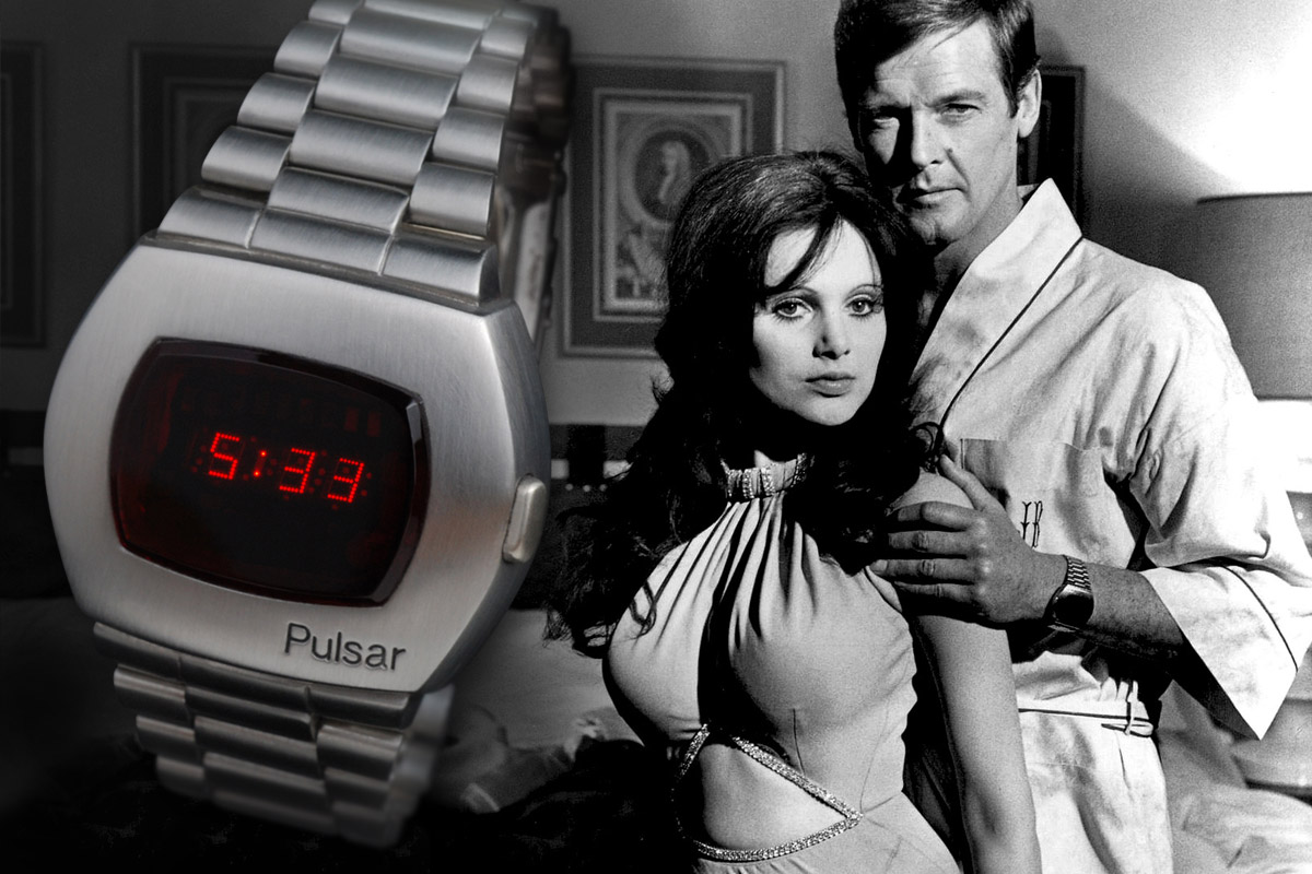 Suitably tasteful 1970s advert for the Hamilton Pulsar digital watch, featuring Roger Moore. No, it’s not being ironic.
Within a few years, LCD technology eliminated the power-hungry drivers and in 1974 Microma launched a watch with all the circuitry on a single chip.
However, taken in context, these proto-SoCs were being developed at the same time as the first microprocessors, but they were not themselves general purpose computing devices. They were simply specialised integrated circuits; today they would be called an application-specific integrated circuit (ASIC).
They can be considered an evolutionary dead-end in the history of SoCs.
The 1980s to the 1990s: the First True SoCs
In the 1980s the personal computing revolution took off. This drove some major developments in SoC technology.
During the 1970s, computer peripherals were typically large, bulky circuit boards full of regularly-arranged 14- and 16-pin logic chips. These chips housed the logic gates (AND, OR, NOR, etc) that decoded the signals from the CPU and encoded the data from the disk drive, tape machine, or whatever.
At first these peripherals were low-volume because the market for personal computing was simply too small. But as the market grew, it made economic sense to integrate more miscellaneous functions onto fewer chips. This is a pattern that started with the development of the integrated circuit and continues to this day.
The resultant chips encapsulated arbitrary chunks of logic and were similar in concept to what today we’d call ASICs. They weren’t systems on chips, but highly integrated circuits.
But the next logical step was to combine this integration on the same silicon die as a CPU. This would allow software to control the chip, and make it far more versatile (and upgradeable).
Many complex peripheral devices were built this way, with microprocessor and DSP (digital signal processor) cores integrated into the same package as some specialist I/O hardware and perhaps memory. The most obvious candidates for this treatment were graphics chips, hard disk controllers and network cards.
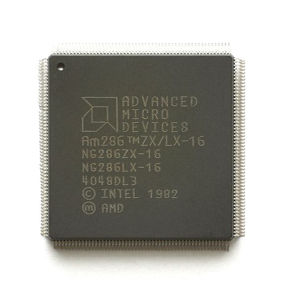
In 1991, AMD released the AMD286ZX/LX family of SoCs. It combined AMD’s 80286-compatible core with all the supporting circuitry of the IBM PC motherboard. This included the bus controller, DMA controller, interrupt controller, and clock generator.
The chip was 100% compatible with the IBM PC-AT board and were for use in the nascent laptop market. It still needed external RAM, BIOS, graphics card and other I/O functions, but it eliminated the need for a large, complex motherboard.
The AMD268ZX/LX devices could certainly be considered the first SoCs in the spirit of how we use the term today. Although they don’t compare to modern SoCs, they really did integrate a huge part of the computer system onto a single chip.
Mid-1990s: the Early GSM Mobile Phone Era
If the personal computer revolution of the 1980s seeded the initial development of system-on-chips, then there was another industry that was to about to cause it to go stratospheric during the 1990s.
The mobile (cell) phone boom was the single biggest driving force behind the development of system-on-chips. I was in the industry at that time and I recall very well how the technology changed so rapidly.
To understand why, let’s start with an extract from an earlier article I wrote on the subject:-
In the early days of GSM, a 2G handset contained maybe a dozen chips, giving rise to famously bulky handsets. Manufacturers had a strong incentive to make them smaller, lighter and less power-hungry.
It goes on to explain why there were so many chips:-
There was a primary CPU to handle the user interface and the upper layers of the GSM protocol stack. This needed quite a lot of RAM, and even more Flash memory for the bespoke operating system, application and protocol code. On top of that was a separate so-called baseband processor in the form of a digital signal processor (DSP), to handle the physical layer of the GSM protocol, including complex, mathematically-intensive operations such as channel coding and speech coding. The baseband also needed its own memory. Then there was the mixed-signal chip, which incorporated the lowest level of modem and radio-frequency (RF) functions.
In addition to this there were a lot of smaller chips to handle various peripheral functions such as audio, keyboard, LCD display, battery charging, etc.
In 1996 I was working for a Japanese company developing one of the early GSM handsets. The first time I saw their “evaluation board” I was flabbergasted: it was a single PCB that must have measured around four square feet!
An eval board is basically a working phone with all the chips laid out so the system can be debugged. It’s not a prototype, it’s the final design, used for software development before the design is shrunk into a handset “form factor” (which may be done by another company altogether). Debugging on the final form factor is much harder, so eval boards are invaluable during development.
The eval board showed how insanely complex the GSM handset was. We were into a new level in consumer electronics: the manufacturers were cramming more and more hardware into smaller and smaller spaces. It was reminiscent of the microprocessor revolution of the 1970s, when the CPU circuit boards of so-called minicomputers were squeezed onto single chips.
Late 1990s: the Dawn of ARM Holdings
The next milestone came with the advent of ARM’s “fabless” processors.
ARM Holdings is a company based in Cambridge, UK, that licenses their processor design to other manufacturers. They were born out of a joint venture between Apple and Acorn Computers.
Acorn was a British company with a history of developing popular computers in the 8-bit days. Later they were known for the Archimedes computer, the first consumer machine to feature an advanced reduced-instruction-set (RISC) processor. But by the mid-1990s, the IBM PC was in full control of the market, and no-one bought the Archimedes any more.
Exiting the personal computer market, and funded by Apple (before Apple’s own financial woes), the remnants of Acorn became ARM and kept hold of their RISC design. And in the late 1990s ARM used it in designs for early SoCs to be used as disk drive controllers.
ARM’s RISC CPU was very powerful and, importantly, much less power-hungry than its competitors. This made it ideal for use in embedded systems, as the disk drive SoC had shown. And it seemed ARM had hit upon a working business model: licensing their CPU design to other manufacturers for them to integrate it into their own silicon.
This turned out to have immense significance for the future of ARM and also for the mobile telecoms market.
Early 2000s: Cheaper, Smaller Phones
Because the ARM processor was a silicon design, rather than a physical lump of silicon, it could be integrated onto a silicon die with just about anything else. This could be memory, I/O, or even other processors. The applications obviously went way beyond disk drive controllers…
Mobile handset manufacturers were still struggling to cram more and more features onto their shrinking PCBs. (Engineers would cry, “What now? A camera? Why?!”)
They took notice of ARM’s unique proposition. Especially its low power use.
A common configuration they came up with was an ARM core , some integrated memory and a DSP core. This solved a whole boatload of integration problems in the GSM world, suddenly enabling handsets to get down to a handful of chips, with the majority of the work done on the power-efficient SoC.
As the SoC become more integrated and efficient, so the handsets grew smaller and the battery life started to rise. Remember tiny phones with standby times of two weeks, a month? They became the norm in the “dumb phone” era, because the processing problem had been solved.
But of course the network providers were launching more complex communications systems. 2.5G came along in the early 2000s which meant more data could be sent via the network. The DSPs grew meatier to cope with the extra physical layer algorithms, but the additional data had to be consumed, so multimedia messaging, music playback and more advanced cameras became common on 2.5G phones. All that extra data had to be processed so the ARM cores got more advanced and the SoC integration continued.
2001: the iPod
In autumn of 2001, in the wake of the 9/11 attacks on the US, a beleaguered and pretty-much written-off Apple launched a new product: the iPod. Marketed as the Walkman for the 21st century, it advertised being able to hold “1000 songs in your pocket.” It had a revolutionary new UI and a focus on slick design that Apple were famous for.
It was based on the PP5002 twin-core ARM SoC from a company called PortalPlayer. The PP5002 was quite interesting: in addition to the two ARM cores and memory, it featured audio processing, an LCD driver, a hard disk controller and battery management on the same silicon die.
For the rest of the decade, Apple would release over 20 models of the iPod, each time adding new features, polishing the design for a perfect multimedia experience.
Mid-2000s: Asian Expansion
Throughout the early 2000s, the market in Asia also grew rapidly. This led to unprecedented demand from huge markets such as China and India. Price point became even more significant in these markets than it was in the west.
By the early 2000s the established far eastern tech giants such as Samsung, LG, and the like, were already manufacturing cheaper mobile handsets specifically for the Asian market.
And a few years later the Chinese market was growing rapidly. Suddenly a lot of companies relatively unknown in the west, such as ZTE and TCL, were buying chipset designs for handsets for local markets.
All of this demanded even cheaper chipsets, a need that was filled by a variety of smaller UK and US companies, such as Qualcomm and Broadcom, and many smaller companies. They sold “reference designs” for virtually the entire mobile handset, based around SoCs with ARM cores and DSPs from a variety of partner companies.
The SoC market was reaching maturity. Companies were well established and the path to the future was set: smaller and smaller handsets, longer battery life, and the slow introduction of new features. Some of the newer phones even had downloadable games… but no-one ever downloaded them.
2007: Revolution! The First iPhone
When the iPhone was launched in 2007 it represented a monumental shift in mobile technology. In a single stroke, Steve Jobs and Apple rewrote the rulebook on developing mobile phone hardware.
It took a little time to sink in though. Things called “smartphones” already existed. The high-end Nokias and SonyEricsson handsets featured email, internet browsing, music and games. Perhaps the most well-established “smartphone” manufacturer was the Canadian company Research In Motion, whose ubiquitous Blackberry devices were the mainstay of business folk and politicians worldwide.
RIM were famously in denial about the iPhone. Their CEO declared that touchscreens would never take off because people wanted to be able to type on a real keyboard. This position is understandable; after all, RIM’s entire business model was to bring business-class, desktop communications to the mobile world. That meant writing emails.
Of course, the iPhone blew them out of the water.
Building upon what they’d created with the iPod, Apple used a Samsung package-on-package that featured an SoC containing an ARM core and a GPU, stacked with 512MB of RAM. They also added a separate baseband SoC consisting of an ARM and DSP from the mobile industry to add cellular and multimedia capability, as well as almost a dozen other complex chips.
The original iPhone chipset included:-
- 32-bit single-core ARM CPU/GPU hybrid called the APL0098 combined with 512MB SDRAM, fabricated by Samsung
- Infineon PMB8876 S-Gold 2 baseband and multimedia processor (which is itself a complete ARM+DSP-based SoC)
- Infineon M1817A11 GSM RF transceiver
- CSR BlueCore4-ROM WLCSP bluetooth modem
- Skyworks RF power amplifier
- Marvell 802.11 WiFi interface
- Wolfsson audio processor
- Broadcom BCM5973A touchscreen processor
- Intel memory chip (32MB Flash NOR plus 16MB SRAM)
- Samsung 4/8/16GB NAND Flash ROM for disk storage
- a 2MP camera
At the time, the sheer amount of hardware and software crammed into the original iPhone was simply unheard of. But the number of chips was almost a reminder of early GSM handsets. Apple now faced the integration issues that the early GSM manufacturers had: in order to stuff more features into the next model, the SoCs had to get more advanced.
2008-2018: Pushing the Limits
So over the next decade, successive generations of iPhone, iPad and competing Android devices pushed the SoC ever-further. The SoCs gained multiple ARM cores, multiple GPU cores, ever-increasing RAM and multimedia processing features.
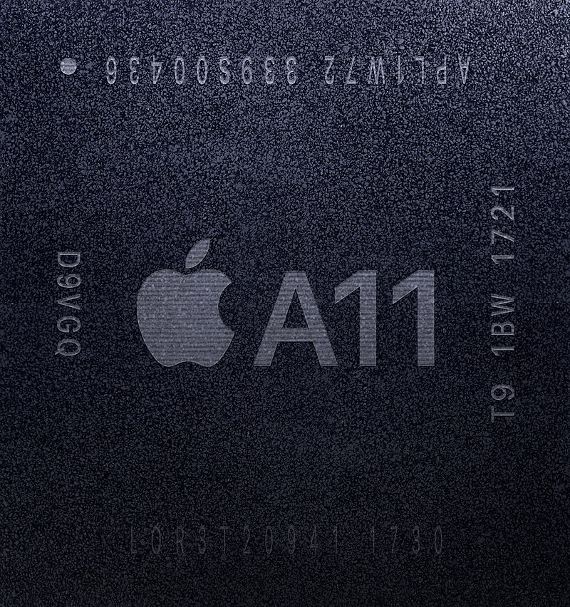
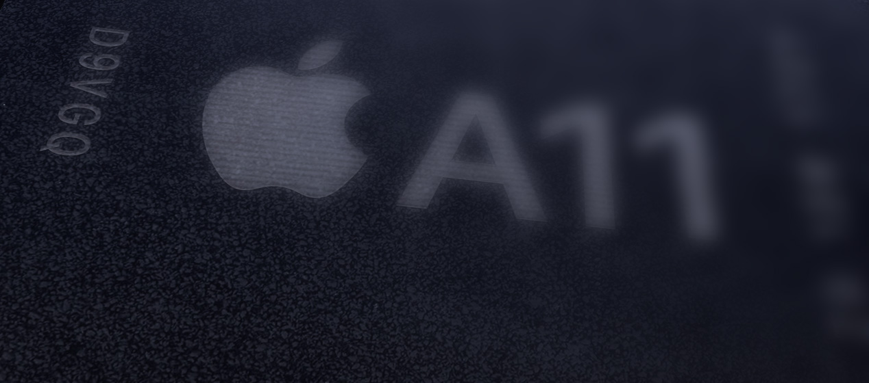
By the time of the iPhone X, the primary SoC (called the A11 Bionic) included:-
- a 6-core 64-bit ARM CPU, 2 of which can run at 2.33 GHz
- a 3-core GPU, used for machine learning tasks as well as graphics
- image processor featuring “computational photography” features (e.g. facial recognition)
- a dedicated neural network engine for machine learning applications
- a motion coprocessor
- an ARM-based “secure enclave” security coprocessor
Again, it is vertically stacked in a PoP with 3GB of SDRAM.
The primary Apple A11 SoC is way more advanced than the APL0098 in the original iPhone. There is a huge amount of image processing, machine learning and multimedia processing going on inside the A11.
Where Next…?
At the time of writing this, the A12X Bionic has just been released. It currently represents the state of the art in system-on-chip technology.
But of course, the level of integration will continue to increase, inevitably following Moore’s Law. I don’t doubt that one day, maybe 10-15 years from now, all the functionality of the iPhone X will be available in a single SoC. And that SoC will be just part of an even larger forest of silicon complexity.
And so the cycle continues.
Get in Touch!
I hope you’ve enjoyed reading this as much as I’ve enjoyed writing it. I’ve tried to cover a lot of ground and I’m sure to have missed stuff out – I’d love to hear form you about any additions or improvements you think I could make, so please contact me if you’ve any feedback.
And if you’d like to hear about my articles when they come out, please join my mailing list.